
![]()
HOME| TEXT| GRADING | STAFF | DEMOS | LECTURES | LABS| ELECTRONICS| PROGRAMS
(Post Production)
|
The *.MAX file that we are using to make the board are an over all view of the board. The company that will produce the boards needs the board broken down into something that can be coded into a machine. So now we will generate the files that need to be transferred. | |
|
Go to Auto -> Back Annotate. This will bring changes made in Layout back into Capture. | |
|
Go to Auto -> Run Post Processor. |
|
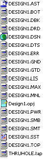
"OK" the next two boxes. They just tell me which file are the "Gerber" (*.GTD) and "Drill tape" (Thruhole.TAP) files, also a "Post Processor Report" (*.LIS). Just close it out. | |||||||||||||
|
Above is a list of all the files just generated, along with my original *.DSN, *.MNL and *.MAX files. | |||||||||||||
|
The company I use will build me a two sided board with no silkscreens. So out of that big list above, here is want they need.
| |||||||||||||
|
The company I use provide software to aid with the transfer of the files. Check the company you will use for details. | |||||||||||||
|
Things not covered in this document can be found in the Layout tutor under help. This points were not need to make this board, but are good to know.
|
Last Modified:
10/04/04
MAE433
WEBMASTER